Perfecting the Surface: How CMP Wafers Improve Wafer Planarization
Wafer planarization is an essential procedure in the semiconductor manufacturing industry. The need for microscopic precision, minute detail, and absolute flawlessness in producing electronic components brings us to the threshold of this remarkable process. The fulcrum of this process lies in achieving surface perfection with Chemical Mechanical Planarization (CMP) wafers.
Through this detailed exploration, we will delve into the essence of wafer planarization, introduce the concept of CMP wafers, examine their chemical and mechanical aspects, and highlight their pivotal role in achieving unparalleled surface perfection. Furthermore, we will explore the advancements in this technology, discuss process control and optimization techniques, and examine their broad range of applications.
Understanding Wafer Planarization
Wafer planarization, also known as wafer polishing, is the process of creating a flat, smooth surface on semiconductor wafers to improve device performance. The process is analogous to sanding a piece of wood until it’s completely smooth; only, in this case, the ‘wood’ is a silicon wafer, and the ‘sanding’ needs to be done at an atomic scale.
Non-uniform wafer topography, or the surface structure, can result in defects that adversely affect the functionality and performance of electronic devices. These defects can be due to the inherent roughness of the wafer surface or the deposition and etching processes used in device fabrication. Hence, achieving a flat and smooth surface is imperative for quality control and enhanced device performance.
Introduction to CMP
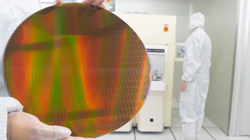
The primary tool used in the wafer planarization process are the CMP wafers. They harness the combined power of chemical action and mechanical abrasion to remove material from the wafer surface and achieve the desired flatness.
The process involves the use of a specially formulated slurry, composed of chemicals and abrasive particles, which is spread over the wafer’s surface. This slurry, in combination with a polishing pad and mechanical action (rotation and pressure), helps remove material from the wafer’s surface, reducing its roughness and non-uniformity.
Chemical Aspects

The chemical components used in these devices play a vital role in planarization. The slurry, composed of a mixture of abrasive particles, chemicals, and water, is key to this process. The abrasive particles, typically silica or alumina, physically abrade the surface, while the chemicals assist in the material removal process.
Adjusting the pH of the slurry can be used to modulate the chemical activity during planarization. For example, changing the pH can influence the rate of material removal and improve the selectivity of the planarization process. Selectivity refers to the ability to remove one material over another, which is crucial in processes such as the planarization of multi-layer structures.
Mechanical Aspects
CMP wafers harness the power of mechanical action in combination with chemical action to achieve planarization. The mechanical aspects involve the use of rotation, pressure, and a polishing pad to physically abrade the wafer surface.
The rotation speed of the wafer and the polishing pad, the applied pressure, and the pad’s hardness can all influence the planarization results. For instance, higher rotation speeds and pressure can increase the rate of material removal but may also lead to higher defect rates. Therefore, optimizing these mechanical parameters is essential to achieving efficient and effective planarization.
Advancements in CMP Wafer Technology
Over the years, significant advancements have been made in CMP wafer technology to improve the planarization results and overall efficiency of the semiconductor manufacturing process. These include the development of advanced polishing pads, more efficient slurry formulations, and innovative abrasive materials.
Polishing pad technology has evolved significantly, with new designs and materials offering improved planarization performance and reduced pad wear. Similarly, advancements in slurry formulations have led to the development of slurries with better selectivity, efficiency, and stability.
Customization and Adaptability
One of the standout features of CMP wafers is their ability to be customized to address specific planarization needs. CMP ones can be tailored for different materials, structures, and device requirements, making them a versatile tool in the semiconductor manufacturing toolkit.
For instance, the choice of slurry can be tailored based on the material to be planarized. Different slurries can offer varying levels of selectivity and efficiency for different materials. Similarly, the polishing pad and mechanical parameters can be adjusted based on the structure and topography of the wafer.
Process Control and Optimization
Process control and optimization play a pivotal role in achieving consistent and repeatable results in CMP wafer planarization. This involves the use of metrology tools and feedback systems to monitor and adjust the planarization process.
Metrology tools are used to measure the surface topography of it before and after planarization, providing vital feedback on the planarization results. This feedback can be used to adjust the planarization parameters, such as the slurry composition, rotation speed, and pressure, to optimize the process and improve the planarization results.
Applications of CMP Wafer Planarization
CMP wafer planarization finds application in various key semiconductor processes. These include interlayer dielectric planarization, shallow trench isolation, and chemical oxide removal, among others.
Interlayer dielectric planarization is used to planarize the dielectric layer between the metal interconnects in multilevel integrated circuits. Shallow trench isolation is a technique used to isolate transistors in modern integrated circuits, and it relies on CMP for the planarization of the isolation trenches. Similarly, chemical oxide removal involves the use of CMP to remove the native oxide layer from the silicon surface.
Challenges and Solutions
While CMP wafer planarization is a powerful technique, it is not without its challenges. Dishing, erosion, and defect formation are some of the issues faced in CMP wafer planarization.
Dishing refers to the excessive removal of material from wide areas, leading to a concave surface. Erosion refers to the excessive removal of material from high areas, leading to a non-uniform surface. Defect formation, such as scratches and pits, can also occur due to the abrasive action of the CMP process.
Various strategies and solutions have been employed to mitigate these challenges. Process optimization, such as adjusting the slurry composition and mechanical parameters, can help reduce dishing and erosion. Material selection, such as the use of softer abrasive particles, can help minimize defect formation.
Industry Standards and Best Practices
Adherence to industry standards and best practices is paramount in CMP wafer planarization. This includes safety protocols, environmental considerations, and quality control measures.
Safety protocols are essential to protect personnel and equipment from the potential hazards of the CMP process, such as chemical exposure and mechanical injuries. Environmental considerations involve the responsible disposal of used slurry and waste materials to minimize environmental impact.
Quality control measures ensure the consistency and reliability of the planarization results. These include the use of metrology tools to monitor the planarization process and the adherence to process control and optimization techniques.
Conclusion
In the realm of semiconductor manufacturing, surface perfection is not just a goal—it’s a necessity. CMP wafers play a critical role in achieving this surface perfection, leveraging the synergy of chemical action and mechanical abrasion to achieve unparalleled planarization results.
As we’ve seen, the journey of CMP wafers is a complex and multifaceted one. It involves an understanding of the chemical and mechanical aspects of the process, the customization and adaptability of the wafers, process control and optimization techniques, and a constant drive to advance the technology and overcome challenges.